AMD Kintex UltraScale+ FPGA KCU116 Evaluation Kit
The Kintex™ UltraScale+™ FPGA KCU116 Evaluation Kit is ideal for evaluating key Kintex UltraScale+ features most notably 28Gbps transceiver performance.
Overview
Product Description
The Kintex™ UltraScale+™ FPGA KCU116 Evaluation Kit is ideal for evaluating key Kintex UltraScale+ features most notably 28Gbps transceiver performance. The Kintex UltraScale+ family provides the best price/performance/watt balance in a FinFET node, delivering the most cost-effective solution for high-end applications.
Key Features & Benefits
- 4x zSFP+ cages to support 28Gbps GTY evaluation
- DDR4 up to 32-bits
- General purpose prototyping elements including FMC, HDMI, PMODs
- PCIe Gen3 x8 compliant
- PCIe Gen4 capable with 3rd party IP or custom IP
Featured AMD Devices
Featuring the Kintex UltraScale+ XCKU5P-2FFVB676E FPGA
| System Logic Cells (K) | 475 |
|---|---|
| DSP Slices | 1,824 |
| Memory (Mb) | 34.9 |
| GTY 32.75 Gb/s Transceivers | 16 |
| I/0 Pins | 304 |

Product Information
Board Features
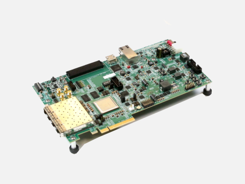
Featuring the KCU116 Evaluation Board
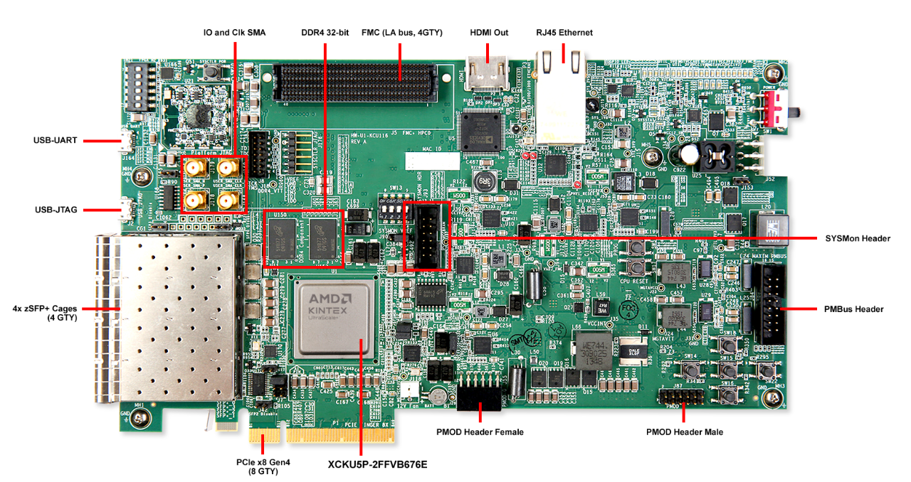
Configuration
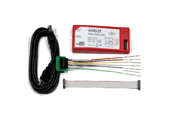
- Onboard JTAG configuration circuitry to enable configuration over USB
- Dual Quad-SPI flash memory provides 2x1 Gb of non-volatile storage
Communication & Networking
- 4x zSFP+ Cages
- 4x SMAs
- UART To USB Bridge
- RJ45 Ethernet connector supporting SGMII Ethernet communications at 10, 100, or 1000 Mb/s
- PCIe Gen3x8 compliant and Gen4 capable
Expansion Connectors
- FMC-HPC (Partial Population) connector (4 GTY Transceiver, 46 single-ended or 23 differential (23 LA pairs: LA[00:22]) user defined signals)
- 2x PMOD headers ( 1 male and 1 female)
Control & I/O
- 5X Directional Push Buttons
- 4X DIP Switches
- PMBUS & System Controller
Memory
- 1 GB 32-bit DDR4 component memory (two [256 Mb x 16] devices) at 1333MHz / 2666Mbpsps
- 64MB (512Mb) Quad SPI Flash
- Micro-SD Card Slot
Clocking
- Dual Si570 Clock chips (User & GT)
- SI5328 Jitter attenuating precision clock
- 2x SMA MGT input clocks
Display
- HDMI video out
- 8x GPIO user LEDs
Power
- 12V wall adapter or ATX
What's Inside
KCU116 Board
Featuring the XCKU5P-2FFVB676E FPGA
Vivado™ Design Suite: Design Edition Voucher Code
Node locked & Device-locked to the XCKU5P FPGA, with 1 year of updates
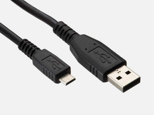
USB Micro Cable
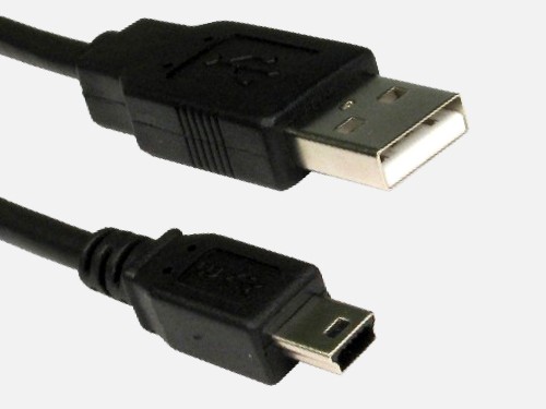
USB Mini Cable
Power Adapter
Power Cord Multiple
Featured Partner
Resources
Design Tools
| Name | Description | License Type |
|---|---|---|
| Vivado Design Suite Design Edition | The AMD Vivado™ Design Suite is a revolutionary IP and System Centric design environment built from the ground up to accelerate the design for FPGAs and SoCs. | Node-locked and device-locked to the XCKU5P FPGA, with 1 year of updates |
| System Controller User Interface (SCUI) | SCUI is a graphical interface that enables users to set and read board parameters such as user clocks, FMC setting and power. | No License required |
| Board Interface Test (BIT) | BIT tests all the board interfaces. | No License required |
Intellectual Property
| Name | Description | License Type |
|---|---|---|
| Memory Interface Generator (MIG) | MIG is a free software tool used to generate memory controllers and interfaces for AMD FPGAs | No-Charge IP |
| DMA for PCI Express (PCIe) Subsystem | The AMD LogiCORE™ DMA for PCI Express® (PCIe) implements a high performance, configurable Scatter Gather DMA for use with the PCI Express 3.x Integrated Block. The IP provides an optional AXI4 or AXI4-stream user interface. | No-Charge IP |


